Foreword
17 years ago, I picked up my first Lego brick. 14 years ago, I built my first K’nex tower. 10 years ago, I wrote my first line of code and blinked my first LED. 6 years ago, I flashed my first FPGA.
These events happened years apart but are somehow part of the same journey; each one a critical piece in shaping how I became an engineer. In many ways, going back in time is like peeling back the layers of abstraction in a computer system, digging deeper and deeper until all that remains is the very thing that makes things tick.
For the longest time, I’ve enjoyed teaching others and passing on the little wisdom I have. No better words on the value of teaching have been said than by Richard Feynman, who neatly encapsulated the entire motivation for this course and others in his quote: “If you want to master something, teach it.” It’s with this spirit that I decided to apply my understanding of ASIC design to a very topical matter and assemble this course. My hope is that by addressing AI we can provide yet another avenue for more hardware engineers to enter this field.
I’m deeply grateful for all the support and mentorship I’ve received from everyone along my engineering journey: teachers, family, friends and work colleagues included. Without them, I never would’ve stepped into the incredibly rewarding world of chip design.
About the author
Matias Wang Silva is a hardware engineer working on custom silicon at Raspberry Pi. He holds a BA and MEng from the University of Cambridge in Electrical and Information Engineering.
He is passionate about teaching curious young minds about engineering topics and has a long history of experience in tutoring.
Introduction
Hardware design is in vogue. If the 2010s were about bringing us great software and cloud, then the 2020s are firmly about the lower layer of the stack, the bare metal. Semiconductor companies like NVIDIA, Intel, and AMD continue to push the limits of technological innovation in the world of AI, spurred on by massive memory and compute demands.
Make no mistake, these are not software companies. According to some, software engineers will evolve to become AI supervisors, merely inspecting and validating the output of AI agents. Hardware engineers on the other hand must understand physics, computer architecture and electronics to create — this set of skills can never be replaced, only augmented.
If that’s not enough to make you jump out of bed or if you’re a diehard softie, there’s the ever famous quote by Alan Kay, inventor of OOP and window-based GUIs:
People who are really serious about software should make their own hardware.
Course objective
The object of this course is to use neural network inference as a vehicle to learn about chip design. The end goal is a fully functional FPGA-based inference engine that can accelerate, in essence, matrix multiplication. This should set you on a good path to understanding the fundamental hardware requirements and constraints of artificial intelligence computations.
Learning outcomes
- Understand the tradeoffs involved in hardware design
- Understand the interaction between the layers of abstraction in computer architecture
- Improve skills in Python, C and SystemVerilog
- Gain hands-on experience with FPGAs, HDLs and Python-based verification
- Gain intuition about machine learning computation and the mathematical operations underpinning them
Deliverable
You will build an inference accelerator on an FPGA. Inference is the process of extracting useful output from a pre-trained neural network, given a set of inputs. This process can be slow and consumes wasteful compute power when run on a CPU. Using FPGAs, we can build hardware accelerators that are custom tailored to this particular type of computation.
Your neural network will be a digit classifier. This is the equivalent of ‘Hello World’ in the AI world. A digit classifier takes an image as an input and outputs 10 numbers, each representing a probability that the image corresponds to a particular number.
You’ll also write a report that conforms to the CREST Gold guidelines
Copyright
All code is MIT licensed. All text is CC BY NC SA 4.0. Figures are mine unless appropriately sourced.
If you’d like to make use of any material here, please contact me at
matias@matiasilva {dot} com. I’m happy to chat!
Prerequisites
This course will not teach you machine learning nor will it teach you how to program. Therefore, the more you know on the below topics, the less confused you will be and the more you will gain from the course.
- Math: linear algebra, in particular matrix multiplication, number systems including binary counting, functions
- Computing: computer architecture, two’s complement, boolean algebra, memory, bit manipulation
- Programming: conditionals and control flow, loops, variables, data types, compilation and linking, logical operators
- Electronics: voltage and current, logic gates, transistors, circuits
- Machine learning: feed-forward fully connected networks, convolutional networks, backpropagation, gradient descent, weights, activation functions, cost functions
- Software: command line familiarity, basic operating systems knowledge, Git
No machine learning or SystemVerilog knowledge is required, learning material will be provided.
For getting to speed with SystemVerilog, I recommend:
- This excellent primer by DJ Greaves from the Cambridge University CS dept.
- This more thorough slide set from Dan Gisselquist over at ZipCPU.
Housekeeping
Work area
All teaching work will take place on a shared server, which students can access at any time. This shared server will host all the tools required to complete the course, including:
- cocotb for Python-based RTL verification
- Icarus Verilog simulator
- Verilator simulator
- yosys for synthesis
- Gowin (FPGA vendor) tools
You will use version control (Git) to manage your codebase in your local area.
VNC port to student mapping
| Username | Display | Port |
|---|---|---|
| neil | :2 | 5902 |
| iris | :3 | 5903 |
| brandon | :4 | 5904 |
| zita | :5 | 5905 |
| michael | :6 | 5906 |
| henry | :7 | 5907 |
| lawrence | :8 | 5908 |
Editor
We will use the VSCode Editor with the Remote SSH plugin to work on files hosted on the shared server.
Course structure
There are 12 contact hours allocated to this project. To meet CREST Gold guidelines, students are expected to make up 58 hours of independent work.
Material has been appropriately portioned into 12 sessions but note that the last few sessions will place emphasis on building and problem solving. In broad strokes, we will learn about:
- training neural networks with PyTorch
- digital design basics
- FPGAs
- machine learning computations
Schedule
We will meet once every weekend, with occasional breaks given for longer term work. Your supervisor will let you know in advance when this happens.
There will be homework set on an ad-hoc basis.
| Date | Duration (hrs) | Time (GMT+0) |
|---|---|---|
| 21/12 | 1 | 8:30 |
| 27/12 | 1 | 9:30 |
| 3/1 | 1.5 | 9:30 |
| 18/1 | 1.5 | 9 |
| 25/1 | 1 | 9 |
| 1/2 | 1.5 | 9 |
| 8/2 | 1 | 9 |
| 14/2 | 1.5 | 9:30 |
| 21/2 | 1 | 9:30 |
| 28/2 | 1 | 9:30 |
Teaching style
While I try and approach all topics from the most intuitive and ‘first-principles’ perspective, it’s possible it might not work for you. I therefore highly encourage the practice of asking questions all throughout the course as well as for you to supplement the course material with some of the resources linked on this site. Remember, this course is not self-contained, it’s merely an introduction to the weird and wonderful world(s) of digital design and machine learning. I encourage you to go off-piste!
A few more tips:
-
Do your homework! I’ve deliberately crafted homework to be direct and short. The more you put in, the more you will get out of it.
-
Do more beyond your homework! You’ll find that as you stretch beyond the scope of the problems I’ve given you, that’s where the real learning will happen. Try something new, break something, extend something, and then tell me about and share it with the class!
-
The classroom is your friend. Imagine sitting in a room with a group of like-minded people with the same interests as you. Sounds great, right? Well, that’s exactly what our classroom is! Please share ideas, thoughts, questions and more with the group. Nothing is worth feeling embarrassed.
-
Embrace discomfort. I will introduce ideas you will never have heard of and it will all seem quite complicated at first. This is fine and intentional. I find that learning works best when you’re thrown in the deep end, made to swim in the ocean as it were.
-
Try first, then ask. You will have to do things you have not done before. This is a fact of learning and I will deliberately put you in these situations. I expect you to use available resources to solve problems and ask me only once you’ve attempted to solve the problem yourself. This benefits the both of us.
And lastly, I will repeat: do not be afraid to ask questions! Interrupt me, please. You may have heard this several times before but I’ll repeat it again: if you’ve got a question, chances are someone has the same one too. Do us all a favor and ask it!
This website
This website is meant to be a digital companion for the course, it is not a replacement. It is highly unlikely you will be able to complete the course relying solely on this website if you are a beginner to digital design.
My explanations are not comprehensive, you should always refer to a textbook for a full description of the topic. The information I give you is motivated by:
- Helping you get to those “aha!” moments
- Filling in the intuition gaps that textbooks miss
- Relevance to our course and what we’re trying to build
I’ve organized the topics and information on each page in accordance with the above guidelines. The goal is that each heading topic motivates the next, in a cascade effect.
A glossary of terms is included at the end of each session to help you in report writing and to avoid any use of imprecise language.
LLM policy
Use of LLMs is highly encouraged as is using resources from outside the course or those I have recommended. If you find something useful, please share it with the class. For completing homework and the final project, all work must be your own.
Session 1: Understanding chip design
Have you ever wondered what powers the millions of electronic devices around you? Which electrical component kickstarted the digital revolution? Starting with transistors, then gates, logic blocks and culminating in entire chips, the semiconductor industry is an amazing feat of humanity. Chips, or Application Specific Integrated Circuits (ASICs), are hidden everywhere: in Huawei cell towers, in Samsung RAM memory controllers, and Apple’s M-series chips. They are so ubiquitous yet they are nearly forgotten and overlooked.
The basics
So, how’s it all done then? First, let’s get some terminology sorted. Chip design, is also known as IC design, IC being short for integrated circuit. You’ll see ASIC thrown around as well, which means the same thing, and expands to application-specific integrated circuit. While ASIC is an all-encompassing term, it is commonly used to distinguish a chip from a general-purpose processor, even though a CPU is itself a kind of ASIC. An ASIC is just a chip that performs one particular task.
Next up, we’ve got EDA. It stands for electronic design automation and refers to the set of software tools that are used to build up circuits, including both analog and digital. Today’s chips are enormously complex; they’re specified at the nanometer level and run at crazy fast speeds (think GHz!). None of this would be possible without both robust commercial and open source tooling.
In this course, we’ll be using open source EDA, mainly because it’s free. Open source and commercial tools exist in a symbiotic relationship. What open source tools lack in funding and manpower, they more than make up for agility and transparency. It turns out that letting bright minds “look inside” does an awful lot of good. Open source tooling won’t help you tape out your next 3nm chip, but they’ll build the engineers that will get you there.
Let’s quick fire a few more:
- Tapeout
- The act of finalizing a chip’s design and committing it for manufacture at a fab
- Fab
- Where highly advanced machinery transforms silicon into full-blown transistors via various processes including etching and lithography. Think TSMC, SMIC, etc.
- Bus
- Refers to any multi-bit vector that carries data with well-defined semantics
- Fabric
- Also called interconnect. The collection of hardware that orchestrates accesses from masters and responses from slaves. Includes arbiters, decoders, crossbars and more.
- 7nm, 3nm
- Process nodes. They stopped carrying any significant physical meaning a while ago and now just denote different advances or steppings in semiconductor manufacturing technology.
- HDL
- Hardware description language. As the name implies, it describes how hardware is laid out and connected. I cannot emphasize how different it is from software.
But anyway, what’s a chip? A chip is just a big circuit that does something. They’re the “pro”“ version of the breadboard constructions that we’re all used to making, operating under a completely different set of constraints due to their manufacturing process. An ASIC might do one thing really well or it might have a whole host of features that in unison carry out a really complex function.
ASICs contain physical logic gates, these are the semi-fundamental building
blocks. The gates together execute logic functions, like A and (B or C), where
A, B, C are all digital inputs with some meaning we assign to them.
Note
Certain manufacturing processes might use only one type of gate, like NAND. Any arbitrary logic function can be made to use NAND operations (DeMorgan’s rule).
The key piece of intuition here is to grasp the layers of abstraction involved. Very roughly, the layers are:
- Electrons
- Transistors (pn junctions)
- Logic gates
- Flops and logic primitives
- Functional blocks, e.g. adders
- Processors/cores
- Systems-on-chip (SoCs)
- Firmware / bare metal code
- Operating Systems
- Userland applications
- Web applications
The second piece of intuition is that it’s all just circuits. We’re designing circuits with logic gates that carry out a particular logic function. This could be anything. For a CPU, it might be an instruction decoder that generates corresponding control signals for the rest of the pipeline, for a hardware accelerator like ours, it’s a robust matrix multiplier (matmul).
This brings us nicely to FPGAs. FPGAs are extremely useful in hardware design. They allow us to, among other things, execute these logic functions at a much higher speed than in simulation. While ASICs and FPGAs provide us with two different ways of executing these functions, underneath it all, they are still the same logic functions.
Example: an inverter
Let’s use an example to tie these concepts together, namely that of an inverter. An inverter takes a logical input signal and produces its complement; a 1 becomes a 0 and a 0 becomes a 1. In boolean algebra, you’ll commonly see a horizontal bar placed above a variable while in code you’ll often see an exclamation mark (!) placed before a variable to indicate its inversion.
So, at the logic gate level of abstraction, we have the following:
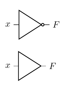
Note
The bottom-most symbol is a buffer, a close sibling of the inverter. It simply produces the same logic level as seen on its input.
Going down one level of abstraction means implementing this logic function with transistors. This can be neatly done using CMOS (Complimentary Metal-Oxide Semiconductor Field Effect Transistor) technology by placing an NMOS transistor after a PMOS and taking the output from the PMOS-NMOS junction.
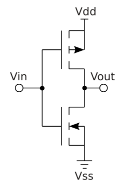
Note
Recall that a MOSFET has a drain, a gate and a source. Conduction from the drain to the source occurs when
V_gate - V_sourceexceeds or is below a certain threshold. PMOS transistors have an n-type channel while NMOS transistors have a p-type channel.This means that for PMOS,
V_gsmust be negative and below the threshold while for NMOS it must be positive and above the threshold. In NMOS transistors, electrons flow while in PMOS transistors it is helpful to think of holes flowing. Refer to Veritasium’s video on transistors for more information.
In this arrangement, a PMOS transistor has its source connected to a positive
supply and its drain connected to the drain of an NMOS whose source is grounded.
The gates of both transistors are connected to a single input V_in. Let’s
observe the circuit behavior with our two state input:
- When the input is low,
V_gsof the NMOS is below 0.7 (typical threshold) while that of the PMOS is deeply negative and below its threshold of -0.7 (PMOS thresholds are negative). PMOS is conducting while NMOS is not. - By the same logic as above, the PMOS stops conducting when the input goes
high and
V_gsbecomes positives and above its threshold. NMOS starts conducting, tying the output to ground.
Of course, there still exists one more layer of abstraction but that is left as an exercise to the reader.
An odd analogy
Over the years, I’ve really found the house analogy useful when drawing parallels between chip design and other processes in the world. A chip is a house. You need a whole team of people to build you a house: the client, the architect, the builders, the building inspector. These are all valid roles in hardware design.
Software is furniture, it can be moved around and different kinds of furniture can coexist as well as be replaced or upgraded entirely. A house needs furniture and as such it must be designed to fit the furniture the client had in mind. It would be absurd to design a house with rooms for 3 fridges, each 3 meters in height, but equally it would be negligent to build a house without room for any fridge at all.
The waterfall model
Chip design follows a roughly sequential process, often called the waterfall model. Each stage builds upon the previous one, and mistakes become exponentially more expensive to fix as you progress further down the pipeline.
Note
This is a highly idealized version. The real world does not work like this…!
Here’s the typical flow:
1. Specification
Everything starts with requirements. What should the chip do? How fast? How much power can it consume? This phase produces a detailed specification document that guides all subsequent work.
2. RTL Design
Register Transfer Level (RTL) design is where we describe the chip’s behavior using hardware description languages like Verilog or VHDL. We’re essentially writing code that describes digital circuits - registers, combinational logic, state machines, etc.
3. Verification
Before committing to silicon, we need to verify that our design actually works as intended. This involves writing testbenches, running simulations, and checking that all corner cases are handled correctly. Industry wisdom says verification takes 2-3x longer than design itself.
4. Synthesis
Synthesis tools take our high-level RTL description and convert it into a netlist of actual logic gates. The tool chooses from a library of standard cells (NAND, NOR, flip-flops, etc.) to implement our design while optimizing for area, power, and timing.
Tip
You’ll see the words power, performance and area a lot. This is called PPA.
5. Place and Route (P&R)
Here’s where things get physical. The P&R tool takes the netlist and actually positions all those gates on the chip die, then routes the metal wires connecting them. This stage must satisfy timing constraints, power delivery requirements, and manufacturing rules.
6. Signoff
Multiple checks ensure the design is ready for manufacturing: timing analysis (does it meet frequency targets?), power analysis (will it overheat?), design rule checks (can the fab actually manufacture this?), and more.
7. Tapeout
The final design files are sent to the fab. There’s no going back after this… you’re committed to manufacturing. If you’ve screwed up, you and your team should hold a diode party once the chip comes back.
This is called “tapeout” from the historical practice of literally sending magnetic tapes to the fabrication facility.
8. Bringup
The chips arrive from the fab! Now comes the moment of truth: powering them on for the first time and seeing if they actually work. Bringup involves testing basic functionality, debugging any issues that slipped through verification, getting firmware running, and validating that the silicon matches your simulations. This phase can range from smooth sailing to months of painful debugging, depending on how thorough your earlier verification was.
The waterfall nature means that finding a bug late in the process is catastrophic. A bug found during RTL design might take hours to fix. The same bug found after tapeout could mean scrapping millions of dollars worth of silicon.
Tools
Becoming familiar with the tools, both commercial and open source, is a must. Here’s a few to remember…
HDLs
Not tools per se but the choice of HDL determines the tools available to you. Advanced tools will have multiple frontends that can parse different HDLs and translate them into some intermediate representation.
The most common HDL is SystemVerilog. Verilog and SystemVerilog used to be different languages but were merged in the IEEE 1800-2009 standard. You might hear references to Verilog 2001 compatible code, since it’s pretty much guaranteed to work with all EDA tools. This refers to the subset of SystemVerilog features available in the IEEE Standard 1364-2001.
In this course, we’ll be using SystemVerilog (2012 version) since it’s what companies actually use. It’s still important for you to know what is and isn’t SystemVerilog since you’ll occasionally have to do some archaeology and dig into some ancient code.
Tip
Why are some features of SystemVerilog not available or implemented by all tools? The reality is that the specification of the language and its implementation are two different tasks, with somewhat competing priorities.
- Verilog/SystemVerilog: The most widely used HDL in industry. C-like syntax, supports both behavioral and structural descriptions
- VHDL: More verbose but strongly typed. Common in aerospace and defense
There’s a different set of languages, specifically DSLs (domain specific languages) that enable a different kind of hardware development. These are so-called high-level HDLs and include Chisel and Amaranth.
Simulation and Verification
- Verilator: Fast, open-source Verilog simulator that compiles to C++
- ModelSim/QuestaSim: Industry-standard commercial simulators from Siemens
- VCS: Synopsys’s commercial simulator, widely used in industry
- Icarus Verilog: Open-source Verilog simulator, good for learning
Synthesis
- Yosys: Open-source synthesis tool, excellent for FPGA and ASIC flows
- Synopsys Design Compiler: Industry standard commercial synthesis tool
- Cadence Genus: Another major commercial synthesis platform
FPGA Tools
- Vivado: Xilinx’s (now AMD) complete FPGA design suite for their devices
- Quartus: Intel’s (formerly Altera) FPGA toolchain
- nextpnr/Project IceStorm: Open-source FPGA place and route tools
Place and Route
- Cadence Innovus: Leading commercial P&R tool
- Synopsys ICC2: Another major commercial option
- OpenROAD: Emerging open-source ASIC flow
Waveform Viewers
- GTKWave: Open-source waveform viewer, works with VCD files from any simulator
- Simvision: Cadence’s waveform viewer
- Surfer: Leading open-source option for waveform viewing
Formal Verification
- SymbiYosys: Open-source formal verification tool built on Yosys
- JasperGold: Cadence’s commercial formal verification platform
The tools in this course will give you a solid foundation in chip design and set you on the right track to working with commercial EDA tools, since the former takes inspiration from the latter (the good bits, at least).
Homework
- Generate a public SSH key and send it to me
- Try and SSH into the shared server
- Download a VNC client and ensure you can access the desktop environment. Make sure to configure your own VNC access beforehand.
- Read through Session 1 to recap content delivered in this session
- Install the VS Code editor and the remote work extension
Accessing the shared teaching server
The teaching server is a simple AMD64 Linux box running Ubuntu 24.04 LTS. You will be asked to hand over your SSH public key. For instructions on creating an SSH key, see this helpful guide.
SSH access
Once your user is set up, you can log in over SSH:
ssh <user>@<edaserver>
Tip
Windows users might want to use PuTTY
You’ll then be handed a shell, into which you can type anything! Try this:
echo "hello, world!"
SSH is a lightweight protocol that runs over TCP, typically on port 22. It allows you to remotely connect to servers and access a shell.
VNC access
You can do plenty on the command line and in fact, I encourage you to stick to the command line as much as possible. That said, for first forays into chip design, having a solid grasp of the GUIs EDA tools offer is of paramount importance.
To access a desktop interface, we’ll be using VNC, which is a remote desktop protocol. The main benefit here is that your windows persist on the teaching server and you can connect at any time you wish to pick up where you last left off.
-
Launch an instance of the VNC server
vncserver :<desktopnum> -geometry 1920x1080 -depth 24 -localhost yesAll students will be assigned a desktop number. Please stick to using only that number.
You might get asked to set a VNC password. Keep this short and memorable, it’s not your main line of defence.
-
Install a VNC client
Use RealVNC’s VNC viewer on macOS and Windows. Or TightVNC, or try both!
-
Forward your VNC port over SSH:
ssh -N -L <port>:localhost:<port> <user>@<edaserver>Your port is 5900 +
<desktopnum>.Forwarding traffic over SSH is a nifty trick for accessing a remote server’s network resource on your local machine. It essentially tunnels all traffic to a port on your local machine over to the remote machine.
Tip
Don’t know what any of these commands or the flags used mean? Use
manfollowed by the command to learn more about the command. Or, ask your favorite LLM.
-
Connect with your VNC client
Your server will be
localhost:<port>and you will be prompted to enter your VNC password.
Misc steps
-
Run this to add the aforementioned open source EDA tools to your
PATH:export PATH="/opt/edatools/oss-cad-suite/bin:$PATH"You are encouraged to add this your
.bashrcfile so thePATHis properly set up in every shell. -
Setting up VNC:
mkdir -p ~/.vnc
nano ~/.vnc/xstartup
Then add the following in your editor:
#!/bin/bash
unset SESSION_MANAGER
unset DBUS_SESSION_BUS_ADDRESS
exec gnome-session
Finally, run:
chmod +x ~/.vnc/xstartup
Session 2: Digital logic primer
Now that we understand what we’re building and roughly how we’re going to do it, let’s dig into some of the fundamentals of digital design.
Binary arithmetic
The binary counting system, or base 2, is much like the decimal counting system we use everyday. As humans, we are no strangers to using a non-decimal counting system. We count our minutes and hours in the sexagesimal counting system, a notion which first originated with the ancient Sumerians. A counting system simply determines how we represent a number, and it is this binary representation that is particularly suitable for computer operations. That’s all there is to it!
The key ideas in binary arithmetic applicable to digital design are:
- There are two states: 1 and 0
- All numbers have an associated bit width. A 4-bit number holds 4 bits. The same is true in decimal but we often conveniently ignore this in basic arithmetic since this limitation is unimportant.
- When a number overflows (eg. the result of 1111 + 1), we roll back to 0. You can think of this as truncated addition, see below.
- 1 + 1 = 0 !
       2³  2²  2¹  2⁰
     ┌───┬───┬───┬───┐
       1   1   1   1    (15)
    +  0   0   0   1    (+1)
     ├───┼───┼───┼───┤
   1 │ 0 │ 0 │ 0 │ 0 │  (0, overflow!)
     └─┬─┴───┴───┴───┘
       │
       └─ Overflow bit (truncated)
Boolean functions
Boolean algebra is a close sister of binary counting, mainly because the 1 and 0 states map nicely onto true and false. True is commonly associated with 1 and false with 0. In boolean algebra, we define a few fundamental operations:
- AND: a.b
- OR: a+b
- XOR: a^b
- NOT: !a
There are a few more, but these are just negations of the above, like NAND !(a.b). I’ve been a bit careless with my syntax above, since I’ve tried to stick to the mathematical notation used for those operations. In software and HDLs, we use a slightly different mixture of symbols to represent the above.
For each operation, we can define a truth table. These enumerate the outputs for all the possible inputs. You’ll notice all operations save for NOT have 2 operands (inputs). Here’s the truth table for AND as an example:
A | B | A AND B
--|---|--------
0 | 0 |   0
0 | 1 |   0
1 | 0 |   0
1 | 1 |   1
Tip
Try and write out the truth tables for all boolean operations
Signed numbers
As computers started to proliferate, we needed a way to represent negative numbers. Remember, all we’ve got is 1s and 0s, you can’t just “add a -” to the start of the number. Eventually, we standardized on a method called two’s complement. There are three ideas we need to apply 2’s complement in our circuits:
- The most significant bit (ie. the leftmost bit) is the sign bit.
- If the sign bit is set, we subtract the number associated with that power of two from the remaining bits.
- To negate a number, we invert all the bits and add 1.
Let’s take an example:
  2³  2²  2¹  2⁰
┌───┬───┬───┬───┐
│ 1 │ 0 │ 0 │ 1 │
└───┴───┴───┴───┘
Interpreting this as an unsigned binary number, we’ve got 9 (8 + 1). If we interpret as signed, this becomes -8 + 1 = -7.
For negation, we have:
 2³  2²  2¹  2⁰
 0   1   1   1   Original: 7
 1   0   0   0   Inverted
 1   0   0   1   +1 = -7
What is digital logic?
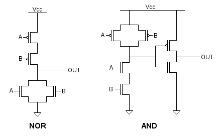
Digital logic is an abstraction built upon fundamental units called logic gates. These gates are themselves made up of switching transistors arranged in special patterns with resistors to achieve the respective binary functions. There is no one strictly correct implementation of a gate, the “best” one will vary according to the specific power, area and performance requirements of the design. Here, we have a generic NOR and AND gate implementation:
The notion of digital is itself part of this transistor-level abstraction. Digital implies binary: 0 or 1, HIGH or LOW, 0V or 5V. However, MOSFETs or BJTs1 can take any allowed voltage within their rated values, which is inherently analog. So, to recap: gates are digital logic components themselves made of “analog” transistors. Of course, the transistors inside gates are chosen for properties that make them particularly suitable for gates, like their voltage transfer characteristics.
Digital logic won over analog logic for various reasons that mostly stem from the fact that having only two allowed states makes circuits easier to design and understand, and therefore lets us turn up the level of complexity of our circuits.
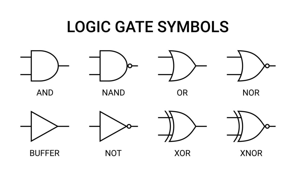
All logic gates implement one boolean function. These are circuits, after all, so it’s useful to have symbols for them:
You might imagine a simple logic function like (A AND B) OR NOT C can be
represented as such:
Tip
Feel free to mess about with the circuit above!
Combinational logic
Combinational logic is formed from boolean functions whose outputs are fully determined by their current inputs. You can achieve quite complex operations using just combinational logic and clever tricks to manipulate bits. These operations execute in zero time, ie. in under 1 clock cycle.
At the lowest level, combinational circuits are built from simple primitives such as NAND gates (in ASIC designs) or LUTs (in FPGA designs). We’ll get to these later; for now, you just need an awareness that how your logic functions are implemented will vary depending on the platform (ASIC or FPGA).
Note
Logic here means the collection of boolean functions that our circuit will implement. It can also refer to the gates, to the different digital components that you might build out of gates, to the HDL code you write and so on. It’s a general term for the thing that your circuit will do.
Karnaugh Maps
A word on Karnaugh maps…While the use of K-maps has mostly been relegated to the classroom and rarely appears in the real-world, it’s an invaluable tool for building intuition on logic reduction.
The main objective is to find the simplest circuit that can model our logic problem. It follows thus that the best solution has the fewest variables in the fewest terms. Recall that a K-map solution can be of the sum-of-products form or product-of-sum form, with the former involving collecting the largest groups of minterms and the latter the maxterms.
Sequential logic
So far, we’ve seen that we can evaluate arbitrary boolean functions using logic gates. However, any meaningful and useful computing system needs a bit more, in particular it needs to store previous values so it can use them in future computations.
The notion of ‘previous’ and ‘current’ require a concept of time. This is called synchronous logic. We say that our circuit is synchronous to a clock, ie. it responds to the clock, most commonly a rising edge (positive edge). A clock signal is a simple square wave with a 50% duty cycle. It is on for 50% of the period and off for the other half.
Tying this all together, we arrive at sequential logic circuits, where the outputs are a function of their current and previous inputs. Flip-flops, also called registers, are used to accomplish this. The simplest flop is a D-flip flop, as shown.

The component above has 3 inputs: clock, d and reset. It has one output q. A
D-flip flop holds the value of the previous input for one clock cycle. D-flip
flops are so common that we simply refer to them as ‘flops’.
Note
Sometimes, you get an additional output which is the inverted version of
Q, since it falls out naturally out of the transistor implementation of a D-flop.
Waveforms
One way to visualize sequential logic circuits is with waveform diagrams, also known as digital timing diagrams, as below.

On the 2nd positive edge of the clock, the input to the flop goes high. The output, however, remains unchanged. One clock cycle later, the flop’s output matches its previous input. Aha, we’ve got 1 cycle’s worth of “memory”!.
This diagram exposes a key understanding of synchronous logic: launching and
sampling/capturing. We say that d is launched on the 2nd clock edge but only
sampled by the flop on the 3rd positive edge. This diagram makes that a bit
clearer by drawing the 0->1 transition of d slightly after the positive edge.
In reality, things are more complicated.
Glossary
- Digital
- Describes a system in which the values are constrained to 1 or 0
- Analog
- Describes a system in which values can span a continuous range
- Logic gate
- An electronic component that implements a logic function
- (Boolean) logic
- A system of reasoning with two values, true and false, that uses operations like AND, OR to combine manipulate statements
- Binary
- Two. A counting system in which only two values are allowed: 1 and 0.
- 2’s complement:
- A way of expressing negative numbers in the binary counting system
-
Metal Oxide Field Effect Transistor, Bipolar Junction Transistor ↩
Session 3: Circuit design and HDLs
Now that we’re firmly in logic territory, let’s explore some useful concepts and RTL1 design patterns.
Multiplexers
A multiplexer, often abbreviated to mux, is a many-to-one circuit that selects one of its inputs to propagate on the output port. It does not modify the chosen input in any way. The select signal can be multiple bits as can the inputs and outputs.
A 2-input mux can be represented by the following Boolean expression:
\[ y = \bar{s} \cdot x_0 + s \cdot x_1 \]
This naturally leads us to a completely plausible logic gate implementation of a mux, though standard cell libraries for a particular process typically have better, more optimized designs.
Muxes can be represented in HDL using if-else statements, case statements, or more commonly with a ternary statement for 2 inputs:
logic foo;
assign foo = condition ? input_0 : input_1;
The ternary statement first evaluates the condition then assigns foo to
input_0 if it is true, otherwise input_1 is assigned. You can chain ternary
statements with parentheses to create >2 input muxes or even cascade two muxes.
SystemVerilog key concepts
To synth or not to synth
You’ve probably noticed by now that SystemVerilog has some awkward constructs for what is meant to be the most used hardware design language. That’s because it wasn’t at the start; SystemVerilog had its origins in Verilog which itself started as a simulation language. The decision to designate a subset of Verilog as synthesizable only came later, when someone had the clever idea of seeing if they could take hardware models and turn them into real hardware.
A consequence of this is a language that is jack of all trades but master of
none and even worse, vendor-dependent. Some tools will try and convert a
non-synthesizable construct into a synthesizable one that kind of works. A good
example is the $clog2() system function that computers the ceiling of log2 for
a particular number, useful to get the number of bits required to encode a
particular number. The IEEE SystemVerilog specification contains the full list
of what is synthesizable and what is not, but that document is over 1000+ pages
and you’re better off learning by experimentation what works and what doesn’t.
Modules
SystemVerilog code is organized into discrete units called modules. You can make a direct equivalence between a module and a circuit on a PCB, it’s something with some inputs and some outputs. They can be immensely useful for splitting up a complex piece of hardware with lots of outputs and core functionality into logical units. It’s important to note, though, that they are just used to establish a hierarchical organizational scheme in SystemVerilog; they do not correspond to physical reality.
There is nothing inherently physically special about a module, it is, at the end of the day, just a collection of combinational and sequential logic with a well-defined input/output interface. When the top SystemVerilog module is synthesized, the tool retrieves all modules instantiated in that file, the modules instantiated by any of those modules, and so on recursively. As you can imagine, designs can grow vastly in gate count and complexity so tools will apply heavy optimization throughout their internal algorithms that begin to blur the module to module boundary.
It’s instead more useful to have the below picture in mind:
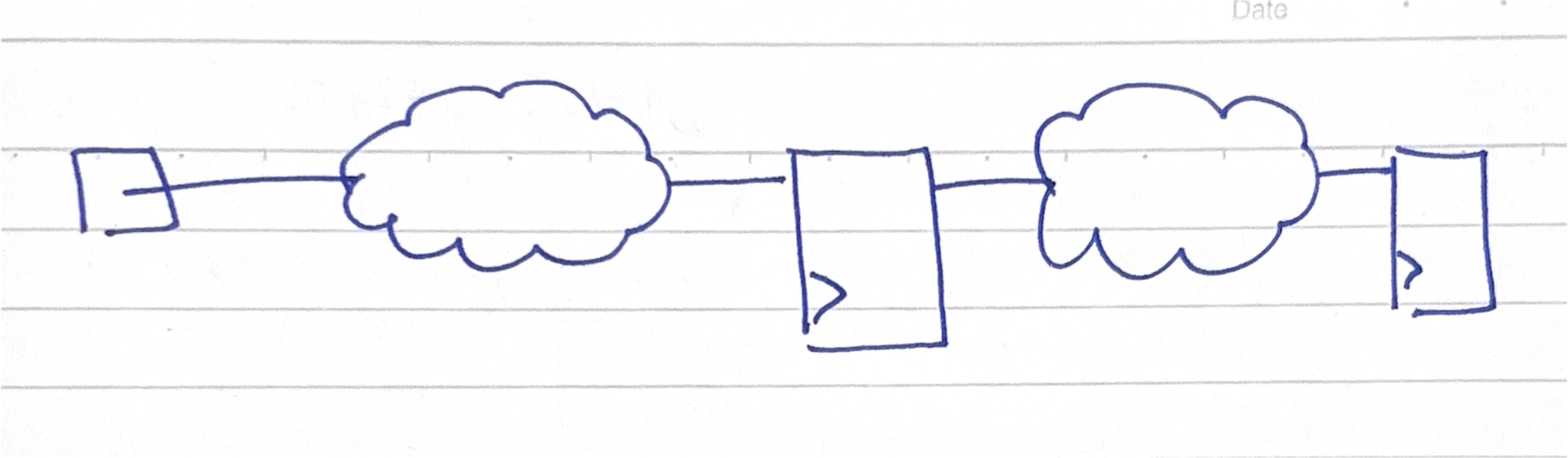
Such a visualization exercise is second nature to the implementation/physical design engineer but is cuneiform to the uninitiated frontend design engineer. The clouds are known as ‘combo logic clouds’ and refer to all the register to register combinational logic lumped up into one unit. This is because a key consideration in chip design is meeting timing, which is characterized by all the delays that plague our various logic primitives.
Altogether, this is a reminder that HDLs are just a tool to describe RTL, another one of our many layers of abstraction, and how we write the RTL has large sway in how the synthesized logic comes out. It’s also a stark reminder of the innumerable concerns involved in chip design and the potential surface area for failure. At the synthesis stage, we’re no longer interested in which module some logic came from (apart from when we need to fix a bug!) and we instead start asking questions like: “which clock domain is this flop in?”, “could we power gate this entire subsystem?”, “what’s the fanout of this gate our lousy design engineer has introduced?” and more. And that’s why a sharp design engineer needs to know that SV modules are just that, modules.
A few more things to note:
- Modules should be kept to one per file, or compilation unit.
- A module can be instantiated multiple times, with
generatestatements enabling powerful and repetitive parameterization. - Name ports meaningfully, they’re the first thing someone sees and how your module appears to the outside world
Keep it logical
Verilog had two synthesizable variable types: wire and reg. In practice, one
used wire, also known as a net, to connect modules together and reg to model
stateful variables that synthesis tools turned into flops. The problem is that
only reg was intended to be used inside procedural blocks which meant that
reg could synthesize to combinational logic in an always block that was not
clocked. Clearly, the name reg is misleading here.
SystemVerilog solved this by removing the distinction between wire and reg
with a new data type called logic and introducing always_comb and
always_ff. This greatly improved design intent, code readability and unlocked
new checks for synthesis tools that were not possible before.
The correct practice nowadays is to use logic everywhere and to also add a
`default_nettype none at the top of compilation units (a file) to prevent
implicit net bugs. You still need wire for multi-driver tristate nets.
State machines
You will come across the term “Finite State Machine” a lot in hardware design. It’s an extremely useful design pattern and one that you will find yourself reaching for constantly in your engineering toolbox.
A state machine is a circuit that has well-defined modes and transitions between those modes which are also well-defined. As with all circuits, we are interested in the inputs and outputs. For a given mode, a state machine will produce some output, which may or may not depend on the current input.
Note
The distinction between a state machine whose output is purely derived from its state is called a Moore machine while one that has its outputs derived from the state and the current input is called a Mealy. In design, this distinction is not really important but its a useful idea to keep in mind.
When it comes to expressing state machines in HDL, we’re really interested in
two things: logic for generating the next state and logic for generating the
output. The only sequential logic is the flops used to store the state. A common
pattern is to express both logic blocks in procedural always blocks with a
case statement.
Warning
Framing a particular design as an FSM and others as not can encourage some binary thinking which is unhelpful and detracts from the point.
A colleague of mine once said: “Matias, everything is a state machine” and there’s truth to that. Ultimately, all sequential logic is stateful; our combinational circuits generate the next state and our flops store the current state, we then output something useful given the input and the current state. Thought of this way, the FSM designs you see around are just one particular way of doing things but by no means the only one. It’s important to make the distinction here between the functionality you’re trying to achieve and the implementation. While FSMs are useful, always consider whether another solution might be more better for PPA, code maintainability or any other objective.
With that out the way, let’s focus on some design considerations:
- State encoding: you need some way to capture symbolic states in binary.
Three at your disposal: binary, one-hot (1-bit per state), or Gray. It’s
usually better to let the synthesis tool figure the best one out for PPA, but
you can explore the effects of each as a useful exercise. Always use
typedef-d SV
enums for your state variables, or if that’s not available alocalparamat the very least. - Case statements: Use
unique caseto catch bugs. Make sure to specify all states in order to prevent inferring a latch. Latches are bad! - Big FSMs: Avoid creating large unwieldy FSMs, they are a nightmare to debug. Instead, split FSMs up into logical chunks that make sense in your design context.
- Keep FSM logic focussed: Do not try and cram in other logic into your FSM procedures just because it’s convenient.
Read this article for a good guide on writing FSMs.
Delays
Setup and hold times
Resets
Homework
Valid solutions must be fully justified.
- This question is about a sequential and combinational logic circuit.
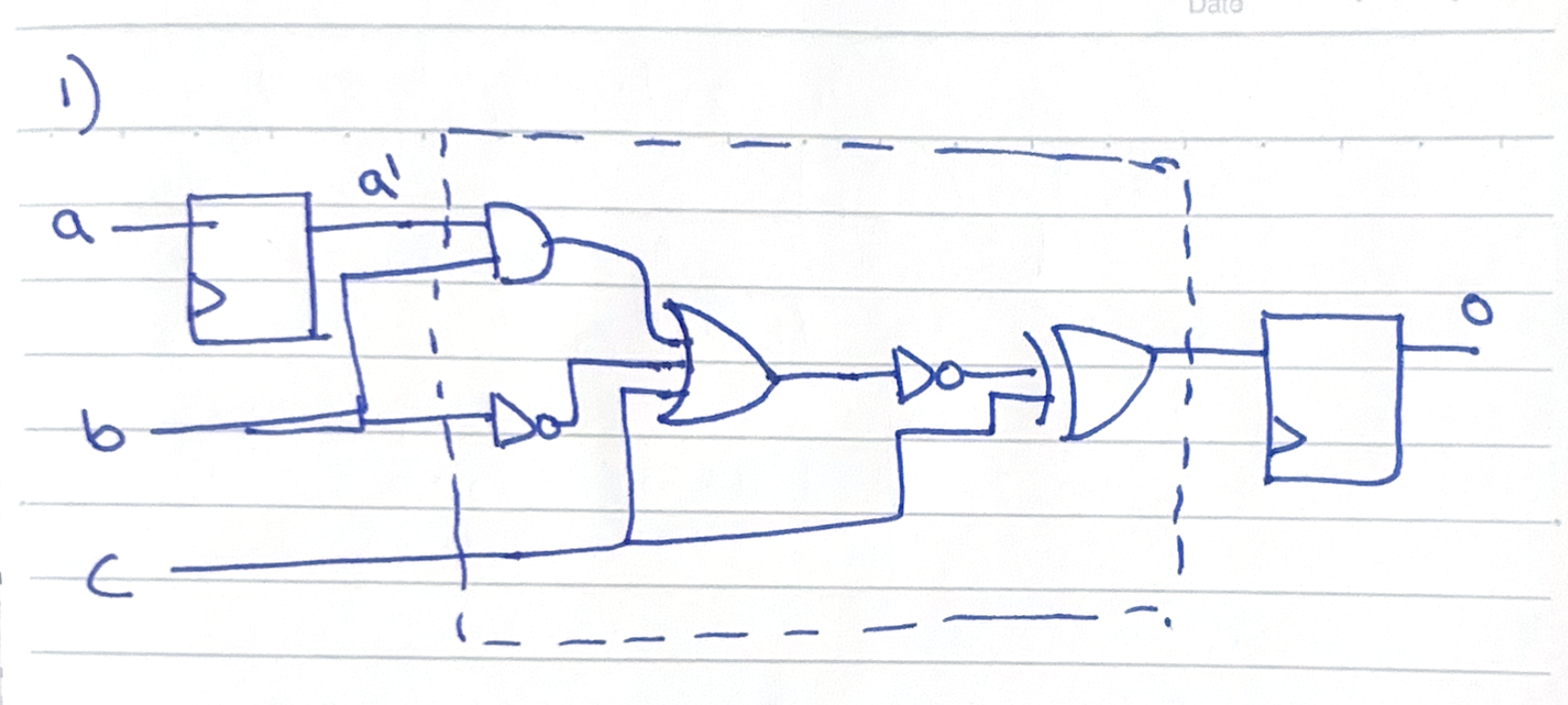
- Write out the truth table for the dashed area, using intermediate variables as required.
- Construct a digital timing diagram for the output
ospanning a total of 10 cycles given the following information about the inputs:
- A is low for the first half and high on the second half of time.
- B toggles every cycle (1 -> 0 -> 1 -> …).
- C is high for all time except on cycles 3 and 4.
- Write valid HDL to model the circuit
- Use a testbench to prove that your answer to part 2 is correct.
- This question is about Boolean expressions and Karnaugh maps
Consider the design of a warning light system that alerts a car user to check their engine. The design requirement is as follows:
A warning light should turn on when:
- The engine is running (A) and oil pressure is low (B), OR
- The engine is running (A) and temperature is high (C), OR
- Both oil pressure is low (B) and temperature is high (C)
- Express the requirement as a Boolean expression.
- Produce the circuit diagram that correctly turns on the light, using Karnaugh maps or otherwise.
- This question is about SystemVerilog.
You are tasked with designing a 4-bit counter that can count up or down, controlled by two corresponding inputs. You should use the skeleton below to guide your answer.
module simple_counter (
    input  logic       clk,
    input  logic       rst_n,
    input  logic       count_up,
    input  logic       count_down,
    output logic [3:0] count
);

  // YOUR CODE HERE!

endmodule
- Add sequential logic that achieves the desired functionality.
- Extend the code to output a signal when the counter has overflowed.
- Use a full adder to draw a circuit diagram for your answer to 1.
- This question is about synchronous circuit design.
Note
Answers to this question will count towards session 2 credits.
You are tasked with creating a 3-bit Gray code counter with T flip-flops and some combinational logic.
A T flip-flop is a different kind of flop to the D-flop we’ve been introduced to so far. It has a toggling output when its input is 1 and holds its previous output when the input is 0. This property makes it very useful for counter design.
Gray code is a number scheme in which consecutive numbers differ by only one bit. The full 3 bit Gray code sequence is available below:
000 -> 001 -> 011 -> 010 -> 110 -> 111 -> 101 -> 100 -> 000
- Write down the number of T-flops required to represent a 3-bit Gray code value.
- Produce the excitation table for the T flip-flop.
An excitation table contains the minimum inputs required to generate the next state given a current state. The three columns should be, in order,
Q,Q_nextandT, whereTis the input to the T-flop.
- Determine the inputs required to the T-flops to achieve the state transitions required by the Gray code sequence
- Using K-maps or otherwise, determine the combinational logic circuits required to generate the correct T-flop inputs
- Draw out the final circuit you have designed
Hint: think of the output of the T-flops as representing the current state. The inputs to the T-flops are determined by the state.
- This question is about writing RTL.
You are tasked with designing a chip that will manage a traffic light controller. The requirements are as follows:
- There are three lights to be displayed, and therefore three output signals: red, amber and green.
- To ensure the smooth flow of traffic, the light should always be green by default.
- If a pedestrian request (input high for 1 cycle for 1 request) is registered, the lights should switch to amber for 3 seconds followed by red for 10 seconds. Further requests during this time are ignored.
- Once a pedestrian request has been honored, both the amber and red lights illuminate for 3 seconds then switch to green.
- Pedestrian requests are only valid if received when the green light is on.
Challenge requirement: There is a cool down period of 10s after the lights have switched to green during which no pedestrian requests can be received to ensure the smooth flow of traffic.
Assume all signals are properly debounced before they are connected to your block.
Your task:
- Draw a state diagram for this task, thinking carefully about how many states you need to implement the controller
- Write RTL for a simple downcounter, you will use this to time transitions between the states
- Implement the traffic light controller
- Write a testbench for your controller, verifying that all states transition per the requirements
Hints:
- Think about how you will incorporate the downcounter to help you transition between states
- Make sure to use a SystemVerilog typedef’d enum for your states
- Use intermediate signals to help you debug your state machine and for code clarity
-
Register Transfer Level, just refers to the HDL we write with an emphasis that we are working at a level of abstraction above the logic gate level ↩
Session 4: Python-based verification
Our work in writing simple SystemVerilog testbenches has hopefully motivated the need for a more robust, error-prone solution that treats verification for what it is: a software problem. This session is therefore dedicated to introducing Python-based verification as well as some basic methodologies for verifying digital designs.
Anatomy of a (co)simulation
SystemVerilog simulation is governed by a complex event loop with 19 separate deltacycles that … Recall that a simulator is just another C program running on your machine and is thus capable of communicating with the outside world through dedicated APIs and protocols. More specifically, simulators conform to a set of standard functions for reading, writing and modifying data called PLI, later GPI and DPI. You can invoke the simulator with compiled shared object files and it is able to interoperate with code you’ve written elsewhere. This concept is called co-simulation.
Combining compiled code in this way works well and is the premise for how Verilator (an open source simulator) is meant to work. However, for verification, especially for early stage prototyping, we’d like something more dynamic and interactive that would massively speed up development cycles. The solution here is to introduce an interpreted language with a host of helpful properties: classes, a loose type system, and an intuitive REPL. One of the many reasons why speed trumps efficiency in verification is that as chips become ever more complex, the state space for tests increases exponentially and pouring time into writing tests that run at near-native speed is a secondary concern to covering more of that vastly large feature/bug space.
Of course, any use of DPI interfaces adds some overhead to each deltacycle, since data must travel back and forth. By using an interpreted language like Python, we’re doubly increasing the overhead since Python must first invoke dedicated C++ functions, called bindings, which themselves hook into DPI with the simulator.
On performance
Note that we’re not that concerned with performance for small designs since a) suites of tests, called regressions, are often run overnight and are not time-bound b) the productivity speedup and feature breadth for verification afforded by Python is worth the penalty in performance.
For larger designs, it’s worth re-thinking your approach either by profiling your Python setup to eliminate the low hanging fruit, investing time into making a non-cycle accurate C++ model of your hardware, writing C++ tests for lengthy and complex tests with lots of DPI, using an emulation hardware stack, or even FPGAs. While the plethora of options might seem like a recipe for decision paralysis, each one comes with its own set of tradeoffs, adding to the beauty of digital verification; it’s a Swiss army knife of tools not a one stop shop.
Session 5: FPGAs
FPGAs are devices that implement programmable digital designs, allowing designers to run their synthesized RTL at speeds that appear native compared to simulation. They’re immensely useful tools during the chip design process, both before and after tape-out.
Note
A note on FPGA terminology: the chip that contains the logic cells and programmable routing is referred to as the FPGA. However, these alone are of little practicality and must be mounted on a development board to be used. The development boards provide external interfaces like USB and SPI flash and are responsible for regulating power to the board as well as providing a crystal for clocking.
This distinction is important; FPGA vendors rarely make their own dev boards and they have different concerns to the user of the FPGA dev board.
As with any circuit component, it’s paramount to know what’s inside in order to best make use of its resources. Internally, FPGAs consist of a sea of look-up tables (LUT), each representing some logic function like ‘x OR y AND z’ and some programmable routing. A LUT is characterized by its number of inputs, so we say 4-LUT or 6-LUT to describe a 4 or 6 input look-up table. LUTs store the truth table of a logic function and by chaining together LUTs in specific arrangements, we can compute vastly large combinational and sequential logic.
Just like with regular ASICs, we use a hardware description language (HDL) like SystemVerilog to can describe the behavior we want our FPGA to ‘execute’ and the FPGA synthesis tool will convert this into thousands of logic functions, which we can then program onto the LUTs in the FPGA. Note that execute is in quotation marks, HDL cannot be ‘run’ in the same sense as code in C or Python can. The FPGA is simply a target for our hardware implementation as are ASICs. ASICs are the ‘real deal’; they compute logic functions using logic gates, while FPGAs compute logic functions by connecting together LUTs containing pre-computed values representing our design that produce equivalent (nearly) behavior.
The logic cell
There are a large number of FPGA varieties and families out there, each targeting its own segment of the market. At their core, though, they all share a good number of fundamental components, the most important of which is the logic cell.
FPGAs contain logic cells in the many thousands and they’re behind the “Gate Array” of FPGA. A logic cell contains a LUT, a bypass mux and a D-flop. Together, these components allow the logic cell to implement sequential or combinational logic. The inputs to the LUT are pre-programmed and come from the bitstream produced by the FPGA synthesis tool.
The TangNano family
Session 6: Neural Networks
This course is interesting because it brings together two incredibly complex and rapidly-advancing topics: digital design and machine learning. Now that we’ve wrapped our heads around a few core concepts in the former space, we’re ready to see how to apply our skills to a novel scenario.
Let’s first remind ourselves of our goal: building an inference accelerator on an FPGA. But what exactly are we going to accelerate?
Deep learning
Deep learning is subcategory in the domain of machine learning, which is itself a subcategory of the field of artificial intelligence. It gains its name from the fact that information travels several layers deep through an arrangement of so-called neurons. It is simply one of many approaches to AI but it is also one that has received tremendous attention in the past decade, in part due to its excellent accuracy.
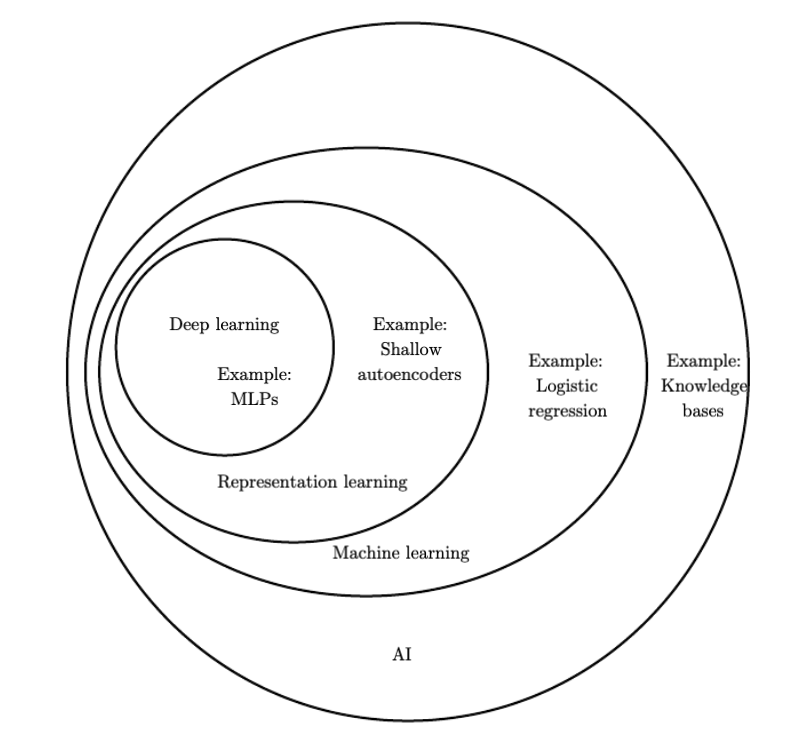
*Figure taken from https://www.deeplearningbook.org/contents/intro.html
Network topologies
The quintessential example of a deep learning model is the feedforward deep network, or multilayer perceptron (MLP). This is also called a fully connected network.
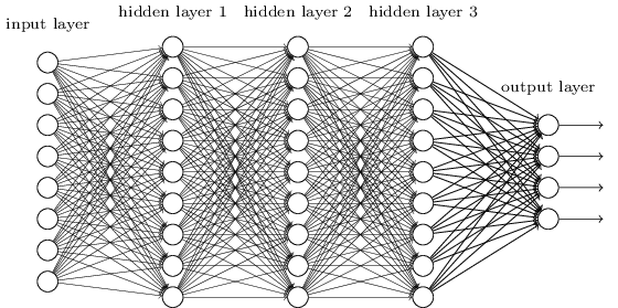
*Figure taken from http://neuralnetworksanddeeplearning.com
A few observations:
- Information travels from left to right
- All neurons in one layer are connected to all neurons in the next
- There is one input and one output layer as well several intermediate “hidden” layers
Another kind of neural network is a convolutional network. We’re going to be building one of these. They’re known for their high accuracy with image inputs due to their awareness of spatial features.
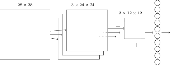
*Figure taken from http://neuralnetworksanddeeplearning.com
The basic structure is as follows:
- Information resident in the 28x28 grid gets gradually reduced to the last output layer with 10 neurons.
- The middle layer is called the convolutional layer and is formed of several feature maps.
- Each feature map is then turned into a unit in the pooling layer.
- Finally, all neurons in the pooling layer are connected to all 10 neurons in the output layer, reminiscent of our fully-connected network.
The ‘convolution’ in the name comes from the fact that the initial operation applied to the image to obtain the feature maps is known as a convolution.
Note
We could, of course, train an MLP and use it for inference. For our relatively well-scoped problem of digit recognition on a 28x28 grid of greyscale pixels, both approaches would work well. That said, MLPs are considered ‘old technology’, having been around for decades before CNNs and are rarely used for image recognition. CNNs themselves were introduced in a seminal paper by LeCun and others in 1998!
Training and inference
Machine learning is a two-step process.
Tip
I’ve found that neural networks can be somewhat of a misnomer. You can draw an equivalence between human neurons firing and being interconnected in a complex web but that’s pretty much where the analogy stops. I’d therefore encourage you to think more in terms of ‘nodes’ or ‘units’ and as the whole system being just a function.
Session 7: Floating point
You may have heard the expression “we’re only as good as our weakest link”. It turns out we can draw a direct parallel between this age-old adage and computer architecture, more precisely that the slowest/least efficient part of a system places an upper bound on its performance. It thus follows that if we’re going to optimize something, we ought to optimize the slowest thing.
Motivation
One of these “slow things” in ASICs is floating point multiplication. This is an interesting example of a type of computation that’s relatively easy to calculate for us humans but quite involved for computers. Most of this is due to limitations imposed by a need to agree on a common standard for representing decimals in binary (IEEE-754). What we gain in standardization we potentially lost in optimization.
Floating point multipliers are logic-heavy, requiring a very large number of adders, and slow, taking potentially multiple cycles to complete one operation. They’re such a common point of speedup that practically every CPU has a floating point coprocessor and the gains to be had are significant! Since design of such a multiplier is potentially a months-long endeavor, we’re going to sidestep this and instead perform all our multiplications with fixed-point numbers.
Primer on floating point
Floating point is a standard way of representing numbers with decimal points in binary. An international standard was defined and can be found as IEEE-754 on the internet.
The key idea behind floating point is that any decimal number can be expressed
as n number of significant digits multiplied by ten to some power m. In a
fixed 32 or 16 bit binary number, n and m are in conflict and are inversely
related. Raising m allows us to represent bigger numbers while a bigger n
gives us greater precision. IEEE-754 defines the following bit arrangement:
Single Precision (32-bit):
┌─┬──────────┬───────────────────────────────────────────────┐
│S│ Exponent │                  Mantissa                     │
│ │  (8 bit) │                  (23 bit)                     │
└─┴──────────┴───────────────────────────────────────────────┘
 1     8                        23
 bit   bits                     bits
\( \int x dx = \frac{x^2}{2} + C \). Programmers first encounter floating
point numbers when they either a) quite literally see the word “float” in their
C programs or b) try and spend hours debugging why 1.5 + 1.5 != 3.0.
Fixed point
Train NN using TensorFlow/PyTorch Train Converge Accuracy > 95%
Load data, define model, train loop, evaluate. You’ll also learn practical things like batch sizes, learning rates, and overfitting
Stanford CS231N
Pipelining convolutions
Memory management
Convolution
Session 8: Architecture and Datapath
In Session 6 we saw how a convolutional network is structured and the kinds of computation involved during training and inference. In this session, we’re going to breaking down the exact data operations required to achieve one successful round of inference. This will allow us write our specification for what we’re going to build.
Session 9: Overview
Session 10: Overview
Session 11: Overview
Session 12: Overview
Extensions
There are a few extensions available for this project:
Creating a digital twin in Python; a computer simulated version of your accelerator. This will allow you to quickly prototype different architecture designs. Improving speed and logic resource utilization, are there any optimizations you can make to your design? Using HLS on a more advanced FPGA. Higher Level Synthesis allow you to program your FPGA in special higher level language, which can speed up design cycles at the cost of losing control over how the design is synthesized.