Session 1: Understanding chip design
Have you ever wondered what powers the millions of electronic devices around you? Which electrical component kickstarted the digital revolution? Starting with transistors, then gates, logic blocks and culminating in entire chips, the semiconductor industry is an amazing feat of humanity. Chips, or Application Specific Integrated Circuits (ASICs), are hidden everywhere: in Huawei cell towers, in Samsung RAM memory controllers, and Apple’s M-series chips. They are so ubiquitous yet they are nearly forgotten and overlooked.
The basics
So, how’s it all done then? First, let’s get some terminology sorted. Chip design, is also known as IC design, IC being short for integrated circuit. You’ll see ASIC thrown around as well, which means the same thing, and expands to application-specific integrated circuit. While ASIC is an all-encompassing term, it is commonly used to distinguish a chip from a general-purpose processor, even though a CPU is itself a kind of ASIC. An ASIC is just a chip that performs one particular task.
Next up, we’ve got EDA. It stands for electronic design automation and refers to the set of software tools that are used to build up circuits, including both analog and digital. Today’s chips are enormously complex; they’re specified at the nanometer level and run at crazy fast speeds (think GHz!). None of this would be possible without both robust commercial and open source tooling.
In this course, we’ll be using open source EDA, mainly because it’s free. Open source and commercial tools exist in a symbiotic relationship. What open source tools lack in funding and manpower, they more than make up for agility and transparency. It turns out that letting bright minds “look inside” does an awful lot of good. Open source tooling won’t help you tape out your next 3nm chip, but they’ll build the engineers that will get you there.
Let’s quick fire a few more:
- Tapeout
- The act of finalizing a chip’s design and committing it for manufacture at a fab
- Fab
- Where highly advanced machinery transforms silicon into full-blown transistors via various processes including etching and lithography. Think TSMC, SMIC, etc.
- Bus
- Refers to any multi-bit vector that carries data with well-defined semantics
- Fabric
- Also called interconnect. The collection of hardware that orchestrates accesses from masters and responses from slaves. Includes arbiters, decoders, crossbars and more.
- 7nm, 3nm
- Process nodes. They stopped carrying any significant physical meaning a while ago and now just denote different advances or steppings in semiconductor manufacturing technology.
- HDL
- Hardware description language. As the name implies, it describes how hardware is laid out and connected. I cannot emphasize how different it is from software.
But anyway, what’s a chip? A chip is just a big circuit that does something. They’re the “pro”“ version of the breadboard constructions that we’re all used to making, operating under a completely different set of constraints due to their manufacturing process. An ASIC might do one thing really well or it might have a whole host of features that in unison carry out a really complex function.
ASICs contain physical logic gates, these are the semi-fundamental building
blocks. The gates together execute logic functions, like A and (B or C), where
A, B, C are all digital inputs with some meaning we assign to them.
Note
Certain manufacturing processes might use only one type of gate, like NAND. Any arbitrary logic function can be made to use NAND operations (DeMorgan’s rule).
The key piece of intuition here is to grasp the layers of abstraction involved. Very roughly, the layers are:
- Electrons
- Transistors (pn junctions)
- Logic gates
- Flops and logic primitives
- Functional blocks, e.g. adders
- Processors/cores
- Systems-on-chip (SoCs)
- Firmware / bare metal code
- Operating Systems
- Userland applications
- Web applications
The second piece of intuition is that it’s all just circuits. We’re designing circuits with logic gates that carry out a particular logic function. This could be anything. For a CPU, it might be an instruction decoder that generates corresponding control signals for the rest of the pipeline, for a hardware accelerator like ours, it’s a robust matrix multiplier (matmul).
This brings us nicely to FPGAs. FPGAs are extremely useful in hardware design. They allow us to, among other things, execute these logic functions at a much higher speed than in simulation. While ASICs and FPGAs provide us with two different ways of executing these functions, underneath it all, they are still the same logic functions.
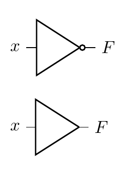
Example: an inverter
Let’s use an example to tie these concepts together, namely that of an inverter. An inverter takes a logical input signal and produces its complement; a 1 becomes a 0 and a 0 becomes a 1. In boolean algebra, you’ll commonly see a horizontal bar placed above a variable while in code you’ll often see an exclamation mark (!) placed before a variable to indicate its inversion.
So, at the logic gate level of abstraction, we have the following:
Note
The bottom-most symbol is a buffer, a close sibling of the inverter. It simply produces the same logic level as seen on its input.
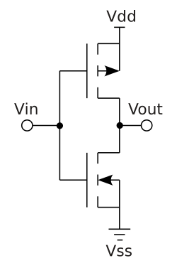
Going down one level of abstraction means implementing this logic function with transistors. This can be neatly done using CMOS (Complimentary Metal-Oxide Semiconductor Field Effect Transistor) technology by placing an NMOS transistor after a PMOS and taking the output from the PMOS-NMOS junction.
Note
Recall that a MOSFET has a drain, a gate and a source. Conduction from the drain to the source occurs when
V_gate - V_sourceexceeds or is below a certain threshold. PMOS transistors have an n-type channel while NMOS transistors have a p-type channel.This means that for PMOS,
V_gsmust be negative and below the threshold while for NMOS it must be positive and above the threshold. In NMOS transistors, electrons flow while in PMOS transistors it is helpful to think of holes flowing. Refer to Veritasium’s video on transistors for more information.
In this arrangement, a PMOS transistor has its source connected to a positive
supply and its drain connected to the drain of an NMOS whose source is grounded.
The gates of both transistors are connected to a single input V_in. Let’s
observe the circuit behavior with our two state input:
- When the input is low,
V_gsof the NMOS is below 0.7 (typical threshold) while that of the PMOS is deeply negative and below its threshold of -0.7 (PMOS thresholds are negative). PMOS is conducting while NMOS is not. - By the same logic as above, the PMOS stops conducting when the input goes
high and
V_gsbecomes positives and above its threshold. NMOS starts conducting, tying the output to ground.
Of course, there still exists one more layer of abstraction but that is left as an exercise to the reader.
An odd analogy
Over the years, I’ve really found the house analogy useful when drawing parallels between chip design and other processes in the world. A chip is a house. You need a whole team of people to build you a house: the client, the architect, the builders, the building inspector. These are all valid roles in hardware design.
Software is furniture, it can be moved around and different kinds of furniture can coexist as well as be replaced or upgraded entirely. A house needs furniture and as such it must be designed to fit the furniture the client had in mind. It would be absurd to design a house with rooms for 3 fridges, each 3 meters in height, but equally it would be negligent to build a house without room for any fridge at all.
The waterfall model
Chip design follows a roughly sequential process, often called the waterfall model. Each stage builds upon the previous one, and mistakes become exponentially more expensive to fix as you progress further down the pipeline.
Note
This is a highly idealized version. The real world does not work like this…!
Here’s the typical flow:
1. Specification
Everything starts with requirements. What should the chip do? How fast? How much power can it consume? This phase produces a detailed specification document that guides all subsequent work.
2. RTL Design
Register Transfer Level (RTL) design is where we describe the chip’s behavior using hardware description languages like Verilog or VHDL. We’re essentially writing code that describes digital circuits - registers, combinational logic, state machines, etc.
3. Verification
Before committing to silicon, we need to verify that our design actually works as intended. This involves writing testbenches, running simulations, and checking that all corner cases are handled correctly. Industry wisdom says verification takes 2-3x longer than design itself.
4. Synthesis
Synthesis tools take our high-level RTL description and convert it into a netlist of actual logic gates. The tool chooses from a library of standard cells (NAND, NOR, flip-flops, etc.) to implement our design while optimizing for area, power, and timing.
Tip
You’ll see the words power, performance and area a lot. This is called PPA.
5. Place and Route (P&R)
Here’s where things get physical. The P&R tool takes the netlist and actually positions all those gates on the chip die, then routes the metal wires connecting them. This stage must satisfy timing constraints, power delivery requirements, and manufacturing rules.
6. Signoff
Multiple checks ensure the design is ready for manufacturing: timing analysis (does it meet frequency targets?), power analysis (will it overheat?), design rule checks (can the fab actually manufacture this?), and more.
7. Tapeout
The final design files are sent to the fab. There’s no going back after this… you’re committed to manufacturing. If you’ve screwed up, you and your team should hold a diode party once the chip comes back.
This is called “tapeout” from the historical practice of literally sending magnetic tapes to the fabrication facility.
8. Bringup
The chips arrive from the fab! Now comes the moment of truth: powering them on for the first time and seeing if they actually work. Bringup involves testing basic functionality, debugging any issues that slipped through verification, getting firmware running, and validating that the silicon matches your simulations. This phase can range from smooth sailing to months of painful debugging, depending on how thorough your earlier verification was.
The waterfall nature means that finding a bug late in the process is catastrophic. A bug found during RTL design might take hours to fix. The same bug found after tapeout could mean scrapping millions of dollars worth of silicon.
Tools
Becoming familiar with the tools, both commercial and open source, is a must. Here’s a few to remember…
HDLs
Not tools per se but the choice of HDL determines the tools available to you. Advanced tools will have multiple frontends that can parse different HDLs and translate them into some intermediate representation.
The most common HDL is SystemVerilog. Verilog and SystemVerilog used to be different languages but were merged in the IEEE 1800-2009 standard. You might hear references to Verilog 2001 compatible code, since it’s pretty much guaranteed to work with all EDA tools. This refers to the subset of SystemVerilog features available in the IEEE Standard 1364-2001.
In this course, we’ll be using SystemVerilog (2012 version) since it’s what companies actually use. It’s still important for you to know what is and isn’t SystemVerilog since you’ll occasionally have to do some archaeology and dig into some ancient code.
Tip
Why are some features of SystemVerilog not available or implemented by all tools? The reality is that the specification of the language and its implementation are two different tasks, with somewhat competing priorities.
- Verilog/SystemVerilog: The most widely used HDL in industry. C-like syntax, supports both behavioral and structural descriptions
- VHDL: More verbose but strongly typed. Common in aerospace and defense
There’s a different set of languages, specifically DSLs (domain specific languages) that enable a different kind of hardware development. These are so-called high-level HDLs and include Chisel and Amaranth.
Simulation and Verification
- Verilator: Fast, open-source Verilog simulator that compiles to C++
- ModelSim/QuestaSim: Industry-standard commercial simulators from Siemens
- VCS: Synopsys’s commercial simulator, widely used in industry
- Icarus Verilog: Open-source Verilog simulator, good for learning
Synthesis
- Yosys: Open-source synthesis tool, excellent for FPGA and ASIC flows
- Synopsys Design Compiler: Industry standard commercial synthesis tool
- Cadence Genus: Another major commercial synthesis platform
FPGA Tools
- Vivado: Xilinx’s (now AMD) complete FPGA design suite for their devices
- Quartus: Intel’s (formerly Altera) FPGA toolchain
- nextpnr/Project IceStorm: Open-source FPGA place and route tools
Place and Route
- Cadence Innovus: Leading commercial P&R tool
- Synopsys ICC2: Another major commercial option
- OpenROAD: Emerging open-source ASIC flow
Waveform Viewers
- GTKWave: Open-source waveform viewer, works with VCD files from any simulator
- Simvision: Cadence’s waveform viewer
- Surfer: Leading open-source option for waveform viewing
Formal Verification
- SymbiYosys: Open-source formal verification tool built on Yosys
- JasperGold: Cadence’s commercial formal verification platform
The tools in this course will give you a solid foundation in chip design and set you on the right track to working with commercial EDA tools, since the former takes inspiration from the latter (the good bits, at least).
Homework
- Generate a public SSH key and send it to me
- Try and SSH into the shared server
- Download a VNC client and ensure you can access the desktop environment. Make sure to configure your own VNC access beforehand.
- Read through Session 1 to recap content delivered in this session
- Install the VS Code editor and the remote work extension
Accessing the shared teaching server
The teaching server is a simple AMD64 Linux box running Ubuntu 24.04 LTS. You will be asked to hand over your SSH public key. For instructions on creating an SSH key, see this helpful guide.
SSH access
Once your user is set up, you can log in over SSH:
ssh <user>@<edaserver>
Tip
Windows users might want to use PuTTY
You’ll then be handed a shell, into which you can type anything! Try this:
echo "hello, world!"
SSH is a lightweight protocol that runs over TCP, typically on port 22. It allows you to remotely connect to servers and access a shell.
VNC access
You can do plenty on the command line and in fact, I encourage you to stick to the command line as much as possible. That said, for first forays into chip design, having a solid grasp of the GUIs EDA tools offer is of paramount importance.
To access a desktop interface, we’ll be using VNC, which is a remote desktop protocol. The main benefit here is that your windows persist on the teaching server and you can connect at any time you wish to pick up where you last left off.
-
Launch an instance of the VNC server
vncserver :<desktopnum> -geometry 1920x1080 -depth 24 -localhost yesAll students will be assigned a desktop number. Please stick to using only that number.
You might get asked to set a VNC password. Keep this short and memorable, it’s not your main line of defence.
-
Install a VNC client
Use RealVNC’s VNC viewer on macOS and Windows. Or TightVNC, or try both!
-
Forward your VNC port over SSH:
ssh -N -L <port>:localhost:<port> <user>@<edaserver>Your port is 5900 +
<desktopnum>.Forwarding traffic over SSH is a nifty trick for accessing a remote server’s network resource on your local machine. It essentially tunnels all traffic to a port on your local machine over to the remote machine.
Tip
Don’t know what any of these commands or the flags used mean? Use
manfollowed by the command to learn more about the command. Or, ask your favorite LLM.
-
Connect with your VNC client
Your server will be
localhost:<port>and you will be prompted to enter your VNC password.
Misc steps
-
Run this to add the aforementioned open source EDA tools to your
PATH:export PATH="/opt/edatools/oss-cad-suite/bin:$PATH"You are encouraged to add this your
.bashrcfile so thePATHis properly set up in every shell. -
Setting up VNC:
mkdir -p ~/.vnc
nano ~/.vnc/xstartup
Then add the following in your editor:
#!/bin/bash
unset SESSION_MANAGER
unset DBUS_SESSION_BUS_ADDRESS
exec gnome-session
Finally, run:
chmod +x ~/.vnc/xstartup