Session 3: Circuit design and HDLs
Now that we’re firmly in logic territory, let’s explore some useful concepts and RTL1 design patterns.
Multiplexers
A multiplexer, often abbreviated to mux, is a many-to-one circuit that selects one of its inputs to propagate on the output port. It does not modify the chosen input in any way. The select signal can be multiple bits as can the inputs and outputs.
A 2-input mux can be represented by the following Boolean expression:
\[ y = \bar{s} \cdot x_0 + s \cdot x_1 \]
This naturally leads us to a completely plausible logic gate implementation of a mux, though standard cell libraries for a particular process typically have better, more optimized designs.
Muxes can be represented in HDL using if-else statements, case statements, or more commonly with a ternary statement for 2 inputs:
logic foo;
assign foo = condition ? input_0 : input_1;
The ternary statement first evaluates the condition then assigns foo to
input_0 if it is true, otherwise input_1 is assigned. You can chain ternary
statements with parentheses to create >2 input muxes or even cascade two muxes.
SystemVerilog key concepts
To synth or not to synth
You’ve probably noticed by now that SystemVerilog has some awkward constructs for what is meant to be the most used hardware design language. That’s because it wasn’t at the start; SystemVerilog had its origins in Verilog which itself started as a simulation language. The decision to designate a subset of Verilog as synthesizable only came later, when someone had the clever idea of seeing if they could take hardware models and turn them into real hardware.
A consequence of this is a language that is jack of all trades but master of
none and even worse, vendor-dependent. Some tools will try and convert a
non-synthesizable construct into a synthesizable one that kind of works. A good
example is the $clog2() system function that computers the ceiling of log2 for
a particular number, useful to get the number of bits required to encode a
particular number. The IEEE SystemVerilog specification contains the full list
of what is synthesizable and what is not, but that document is over 1000+ pages
and you’re better off learning by experimentation what works and what doesn’t.
Modules
SystemVerilog code is organized into discrete units called modules. You can make a direct equivalence between a module and a circuit on a PCB, it’s something with some inputs and some outputs. They can be immensely useful for splitting up a complex piece of hardware with lots of outputs and core functionality into logical units. It’s important to note, though, that they are just used to establish a hierarchical organizational scheme in SystemVerilog; they do not correspond to physical reality.
There is nothing inherently physically special about a module, it is, at the end of the day, just a collection of combinational and sequential logic with a well-defined input/output interface. When the top SystemVerilog module is synthesized, the tool retrieves all modules instantiated in that file, the modules instantiated by any of those modules, and so on recursively. As you can imagine, designs can grow vastly in gate count and complexity so tools will apply heavy optimization throughout their internal algorithms that begin to blur the module to module boundary.
It’s instead more useful to have the below picture in mind:
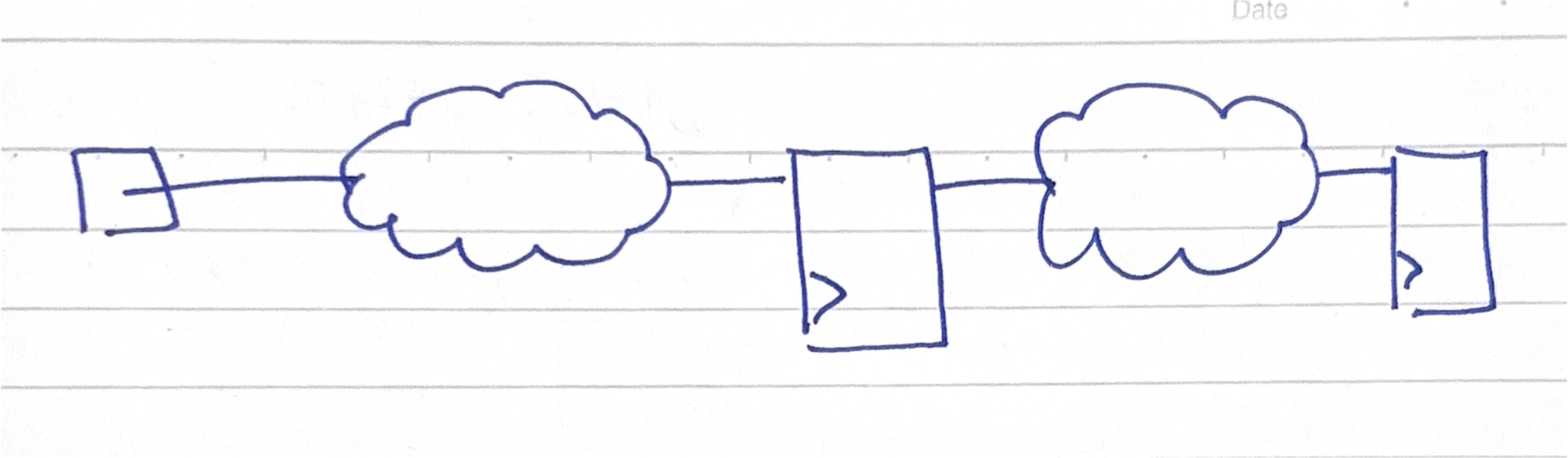
Such a visualization exercise is second nature to the implementation/physical design engineer but is cuneiform to the uninitiated frontend design engineer. The clouds are known as ‘combo logic clouds’ and refer to all the register to register combinational logic lumped up into one unit. This is because a key consideration in chip design is meeting timing, which is characterized by all the delays that plague our various logic primitives.
Altogether, this is a reminder that HDLs are just a tool to describe RTL, another one of our many layers of abstraction, and how we write the RTL has large sway in how the synthesized logic comes out. It’s also a stark reminder of the innumerable concerns involved in chip design and the potential surface area for failure. At the synthesis stage, we’re no longer interested in which module some logic came from (apart from when we need to fix a bug!) and we instead start asking questions like: “which clock domain is this flop in?”, “could we power gate this entire subsystem?”, “what’s the fanout of this gate our lousy design engineer has introduced?” and more. And that’s why a sharp design engineer needs to know that SV modules are just that, modules.
A few more things to note:
- Modules should be kept to one per file, or compilation unit.
- A module can be instantiated multiple times, with
generatestatements enabling powerful and repetitive parameterization. - Name ports meaningfully, they’re the first thing someone sees and how your module appears to the outside world
Keep it logical
Verilog had two synthesizable variable types: wire and reg. In practice, one
used wire, also known as a net, to connect modules together and reg to model
stateful variables that synthesis tools turned into flops. The problem is that
only reg was intended to be used inside procedural blocks which meant that
reg could synthesize to combinational logic in an always block that was not
clocked. Clearly, the name reg is misleading here.
SystemVerilog solved this by removing the distinction between wire and reg
with a new data type called logic and introducing always_comb and
always_ff. This greatly improved design intent, code readability and unlocked
new checks for synthesis tools that were not possible before.
The correct practice nowadays is to use logic everywhere and to also add a
`default_nettype none at the top of compilation units (a file) to prevent
implicit net bugs. You still need wire for multi-driver tristate nets.
State machines
You will come across the term “Finite State Machine” a lot in hardware design. It’s an extremely useful design pattern and one that you will find yourself reaching for constantly in your engineering toolbox.
A state machine is a circuit that has well-defined modes and transitions between those modes which are also well-defined. As with all circuits, we are interested in the inputs and outputs. For a given mode, a state machine will produce some output, which may or may not depend on the current input.
Note
The distinction between a state machine whose output is purely derived from its state is called a Moore machine while one that has its outputs derived from the state and the current input is called a Mealy. In design, this distinction is not really important but its a useful idea to keep in mind.
When it comes to expressing state machines in HDL, we’re really interested in
two things: logic for generating the next state and logic for generating the
output. The only sequential logic is the flops used to store the state. A common
pattern is to express both logic blocks in procedural always blocks with a
case statement.
Warning
Framing a particular design as an FSM and others as not can encourage some binary thinking which is unhelpful and detracts from the point.
A colleague of mine once said: “Matias, everything is a state machine” and there’s truth to that. Ultimately, all sequential logic is stateful; our combinational circuits generate the next state and our flops store the current state, we then output something useful given the input and the current state. Thought of this way, the FSM designs you see around are just one particular way of doing things but by no means the only one. It’s important to make the distinction here between the functionality you’re trying to achieve and the implementation. While FSMs are useful, always consider whether another solution might be more better for PPA, code maintainability or any other objective.
With that out the way, let’s focus on some design considerations:
- State encoding: you need some way to capture symbolic states in binary.
Three at your disposal: binary, one-hot (1-bit per state), or Gray. It’s
usually better to let the synthesis tool figure the best one out for PPA, but
you can explore the effects of each as a useful exercise. Always use
typedef-d SV
enums for your state variables, or if that’s not available alocalparamat the very least. - Case statements: Use
unique caseto catch bugs. Make sure to specify all states in order to prevent inferring a latch. Latches are bad! - Big FSMs: Avoid creating large unwieldy FSMs, they are a nightmare to debug. Instead, split FSMs up into logical chunks that make sense in your design context.
- Keep FSM logic focussed: Do not try and cram in other logic into your FSM procedures just because it’s convenient.
Read this article for a good guide on writing FSMs.
Delays
Setup and hold times
Resets
Homework
Valid solutions must be fully justified.
- This question is about a sequential and combinational logic circuit.
- Write out the truth table for the dashed area, using intermediate variables as required.
- Construct a digital timing diagram for the output
ospanning a total of 10 cycles given the following information about the inputs:
- A is low for the first half and high on the second half of time.
- B toggles every cycle (1 -> 0 -> 1 -> …).
- C is high for all time except on cycles 3 and 4.
- Write valid HDL to model the circuit
- Use a testbench to prove that your answer to part 2 is correct.
- This question is about Boolean expressions and Karnaugh maps
Consider the design of a warning light system that alerts a car user to check their engine. The design requirement is as follows:
A warning light should turn on when:
- The engine is running (A) and oil pressure is low (B), OR
- The engine is running (A) and temperature is high (C), OR
- Both oil pressure is low (B) and temperature is high (C)
- Express the requirement as a Boolean expression.
- Produce the circuit diagram that correctly turns on the light, using Karnaugh maps or otherwise.
- This question is about SystemVerilog.
You are tasked with designing a 4-bit counter that can count up or down, controlled by two corresponding inputs. You should use the skeleton below to guide your answer.
module simple_counter (
    input  logic       clk,
    input  logic       rst_n,
    input  logic       count_up,
    input  logic       count_down,
    output logic [3:0] count
);

  // YOUR CODE HERE!

endmodule
- Add sequential logic that achieves the desired functionality.
- Extend the code to output a signal when the counter has overflowed.
- Use a full adder to draw a circuit diagram for your answer to 1.
- This question is about synchronous circuit design.
Note
Answers to this question will count towards session 2 credits.
You are tasked with creating a 3-bit Gray code counter with T flip-flops and some combinational logic.
A T flip-flop is a different kind of flop to the D-flop we’ve been introduced to so far. It has a toggling output when its input is 1 and holds its previous output when the input is 0. This property makes it very useful for counter design.
Gray code is a number scheme in which consecutive numbers differ by only one bit. The full 3 bit Gray code sequence is available below:
000 -> 001 -> 011 -> 010 -> 110 -> 111 -> 101 -> 100 -> 000
- Write down the number of T-flops required to represent a 3-bit Gray code value.
- Produce the excitation table for the T flip-flop.
An excitation table contains the minimum inputs required to generate the next state given a current state. The three columns should be, in order,
Q,Q_nextandT, whereTis the input to the T-flop.
- Determine the inputs required to the T-flops to achieve the state transitions required by the Gray code sequence
- Using K-maps or otherwise, determine the combinational logic circuits required to generate the correct T-flop inputs
- Draw out the final circuit you have designed
Hint: think of the output of the T-flops as representing the current state. The inputs to the T-flops are determined by the state.
- This question is about writing RTL.
You are tasked with designing a chip that will manage a traffic light controller. The requirements are as follows:
- There are three lights to be displayed, and therefore three output signals: red, amber and green.
- To ensure the smooth flow of traffic, the light should always be green by default.
- If a pedestrian request (input high for 1 cycle for 1 request) is registered, the lights should switch to amber for 3 seconds followed by red for 10 seconds. Further requests during this time are ignored.
- Once a pedestrian request has been honored, both the amber and red lights illuminate for 3 seconds then switch to green.
- Pedestrian requests are only valid if received when the green light is on.
Challenge requirement: There is a cool down period of 10s after the lights have switched to green during which no pedestrian requests can be received to ensure the smooth flow of traffic.
Assume all signals are properly debounced before they are connected to your block.
Your task:
- Draw a state diagram for this task, thinking carefully about how many states you need to implement the controller
- Write RTL for a simple downcounter, you will use this to time transitions between the states
- Implement the traffic light controller
- Write a testbench for your controller, verifying that all states transition per the requirements
Hints:
- Think about how you will incorporate the downcounter to help you transition between states
- Make sure to use a SystemVerilog typedef’d enum for your states
- Use intermediate signals to help you debug your state machine and for code clarity
-
Register Transfer Level, just refers to the HDL we write with an emphasis that we are working at a level of abstraction above the logic gate level ↩